Virgin Boards - PCBs With A Middle Layer
SMD assemblies can not exist without peripheral connection technology.
Meanwhile, there are already some surface assembly component connectors, yet there are still components which must be manually inserted onto a SMD board, then subsequently soldered using either reflow soldering or a selective soldering system.
This means a second processing step is needed in the assembly of SMD components. All additional steps involved, ranging from job preparation, actual placement to final second quality check are carried out.
In addition, documentation obligations need to fulfil ISO regulations.


Development Goal
The goal in the development of our Virgin boards was that our customers can completely save this second processing step and assemblies are only required to be printed with solder paste, then all the conventional components inserted, then on the other side automatic SMD assembly can be accomplished by using a pick and place system.
We have reached the goal!
The Implementation
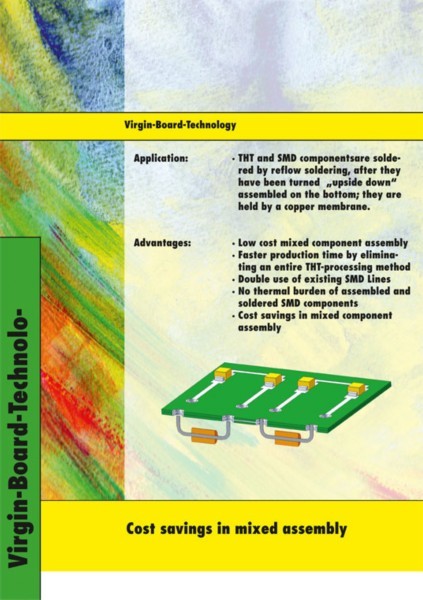
The task was to develop a method where the components are mechanically held in the board, after the placement they can no longer fall out and the PCB can now be flipped 180°.
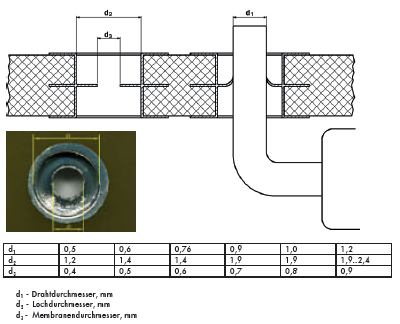
The idea was to introduce a thin copper membrane into the center of the drill holes that gives the component after assembly a mechanical support. From this idea we developed PCB with a middle layer.
This is very unusual, because 3-layer or 5 layer as well as other odd-layer PCBs are not common. In the simplest case, a 3-layer PCB consists of two outer layers and a middle layer:


The Middle Layer
The middle layer acts as a membrane layer in the drilled hole. It is furnished with a drilled hole whose diameter must be smaller than the connections of the conventional
component.
Through extensive experiments we have determined the appropriate drilled hole diameters for all standard conventional components. The following table shows some examples of these values.
Everything In One Workflow
Once the copper membrane on the PCB is pierced with the inserted conventional component the copper membrane is accordingly widened by the wire, thereby creating a barb effect.
The component wire is anchored into the membrane. The component slipping out of the holes is prevented.


The Practical Flow
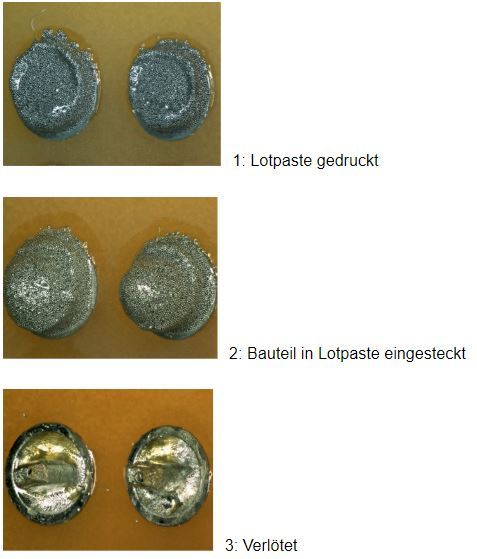
First, the Virgin-Board is printed with solder paste. For this purpose, a standard automatic solder paste dispenser is used, in a single step all SMD pads and the membrane holes are covered with solder paste.
Subsequently, the PCB is removed from the solder paste dispenser and brought to the conventional assembly area. For this purpose, a linked transport system can be expanded to discharge the PCBs after printing. The board is now ready to be flipped and fitted with conventional components.
When placing the connecting wires a portion of the solder paste will hang on the components. This is however an intentional effect, because the solder paste additionally insures that the components are safely maintained in place in the membrane holes.
The PCB is once again flipped over and brought to the automated pick and place area. During the SMD placement the conventional Components hang „upside“ down. This is followed by the reflow soldering of all assembled components.
Advantages
The economic advantage of this method is clearly the cost savings in the operations which are no longer needed.
The slightly higher price of using Virgin-board technology is cancelled out by omitting steps which are not necessary in the production. Neither a selective solder, nor a conventional assembly with subsequent reflow soldering are cheaper.
The Virgin-board technology brings however, not only monetary benefits, but also in technical regard. Extensive tests have shown that in highly thermally dissipating components the usual danger of cold solder joints is reduced to zero, because by the immediate contact of the connecting wire to the copper membrane air gaps are excluded in the solder joint.
The mechanical strength between pad and PCB is greater by a multiple.


